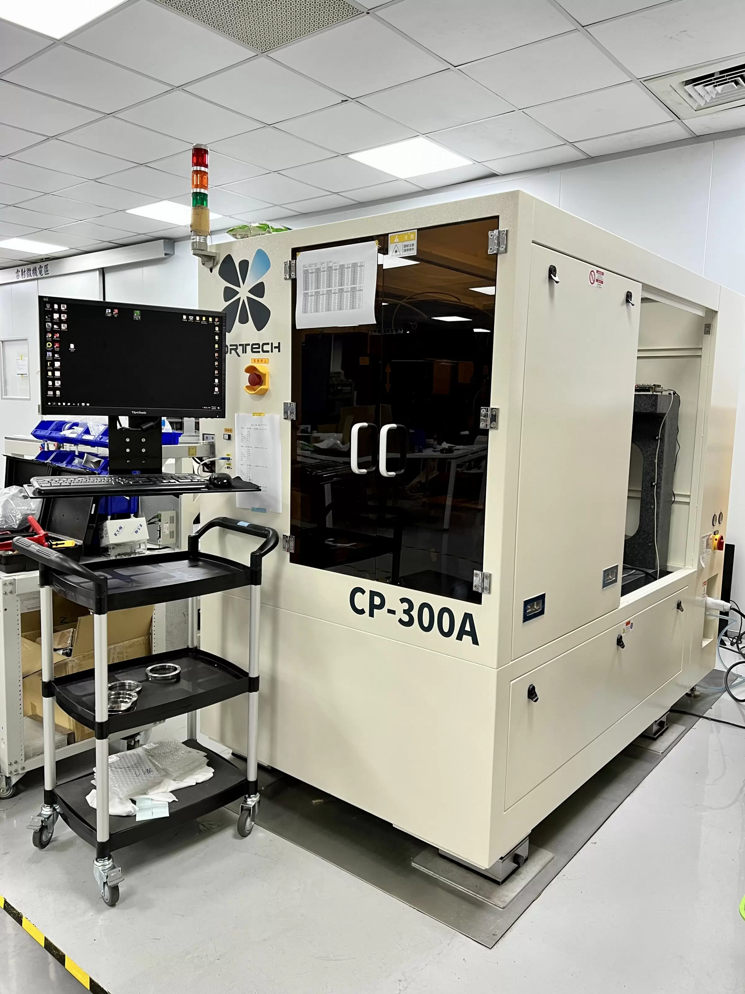
Wafer Fabrication & Semiconductor Packaging | Laser Processing Services & Custom Designed Machines Manufacturer | Hortech Co.
Advanced micron electromechanical packaging for back-end semiconductor process. The precision of the semiconductor front-end process is at the nanometer level, so it belongs to the nanoelectromechanical field. Hortech specializes in micron precision, which is ahead of the advanced packaging industry. The latter focuses on precision at the micron level. Hortech Co. is a high-quality Wafer Fabrication & Semiconductor Packaging, Micron laser processing, precision laser processing, laser etching, laser cutting, laser drilling, laser engraving, laser machines, laser equipment, wafer dicing, wafer drilling manufacturer from Taiwan since 2006. With more than 27 years experience, Hortech Co. is professional provider of laser equipment and OEM solutions.
Wafer Fabrication & Semiconductor Packaging
Advanced micron electromechanical packaging for back-end semiconductor process
The precision of the semiconductor front-end process is at the nanometer level, so it belongs to the nanoelectromechanical field. Hortech specializes in micron precision, which is ahead of the advanced packaging industry. The latter focuses on precision at the micron level.
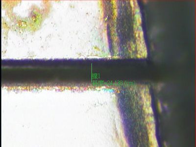
SiC Wafer Dicing
Hortech has developed the ultrafast laser machine that can implement SiC wafer dicing at high...
Details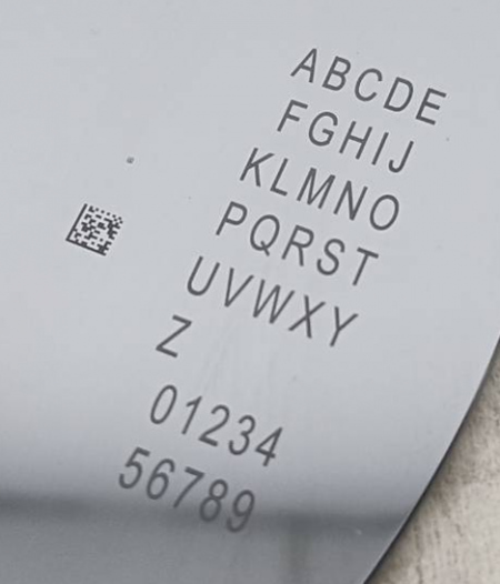
Wafer Laser Micro-engraving
Before processing semiconductor wafers, it is necessary to precisely engrave the SEMI OCR fonts...
Details
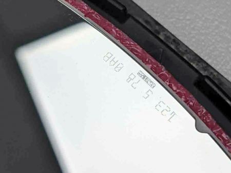
Laser Micro-cutting Small Wafers
The surface of the wafer must be clean and dust-free after the larger one is cut, so it is crucial...
Details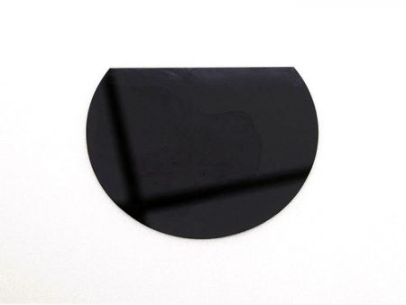
Laser Heterotypic Cutting on Silicon Wafer
Silicon wafers have been widely adopted, so many semiconductor-related industries prefer to use these...
Details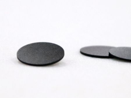
Laser Micro-cutting Fingerprint IC Substrates
To cut fingerprint IC substrates, Hortech coats substrates with protective films to reduce...
Details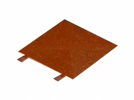
Surface Micro-texturization of Copper Cooling Fins
The surface of copper cooling fins needs to be micro-texturized/micro-structured. Many metal...
Details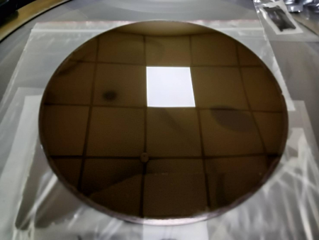
Laser Micro-drilled Silicon Wafer
Material: Si, SiN, and other MEMS wafers. The diameter is: > 5 um
DetailsHot Products
Wafer Fabrication & Semiconductor Packaging | Laser Processing Services & Custom Designed Machines Manufacturer | Hortech Co.
Located in Taiwan since 2006, Hortech Company has been a manufacturer providing precision laser processing services and custom designed machines. Its core techniques include: Wafer Fabrication & Semiconductor Packaging, laser micro-etching, micro-drilling, micro-cutting, and laser engraving. It has successfully developed products for diverse industries, including optical scales for factory automation and robotics, superfine reticles for the defense industry, and wafer dicing and drilling for the semiconductor industry. Hortech's laser OEM/ODM services have served industrial partners from around the world.
Hortech Company was established by Dr. Owen Chun Hao Li in 2016. It has developed a laser marking system used for the traceability of medical circuit boards for a Taiwanese circuit manufacturer in 2018. It has developed the triple wavelength laser combined machining system for a Singapore manufacturer in 2017. It produced different types of magnetic and optical scales with high accuracy for encoders and actuators since 2019. Hortech kept upgrading its laser machines and expanding its services to different regions. Its rigorous quality control processes ensures its clients' needs are satisfied.
Hortech Co. has been offering customers ultra-precision laser machining services and laser CNC machines since 2006, both with advanced technology and 27 years of experiences, Hortech Co. ensures each customer's demands are met.